
What is the minimum trace width for a PCB prototype?
minimum trace width for a PCB prototype
The minimum trace width for a PCB prototype is an important consideration in the design and manufacturing process, as it directly affects the performance, reliability, and manufacturability of the circuit board. In printed circuit board (PCB) design, traces are the conductive paths that connect different components on the board. The trace width, or the width of these conductive paths, is determined by several factors, including the amount of current that needs to pass through the trace, the type of material used for the PCB, the temperature rise that can be tolerated, and the limitations of the manufacturing process. Ensuring the correct trace width is crucial for ensuring that the PCB prototype functions as intended and meets electrical and thermal requirements.
The minimum trace width for a PCB prototype is primarily determined by the current-carrying capacity of the trace. Each trace on the PCB must be wide enough to carry the expected current without overheating or causing excessive voltage drops. If the trace width is too narrow for the amount of current, the trace could overheat, which may lead to thermal damage, component failure, or even short circuits. On the other hand, traces that are too wide take up unnecessary space on the board and increase the cost of the pcb prototype due to the larger area of copper required. Therefore, selecting the correct trace width is essential for balancing electrical performance with space constraints.
To calculate the minimum trace width, designers typically use standards and guidelines such as the IPC-2221 or IPC-2222, which provide industry-recognized formulas and tables for determining the trace width based on the current load, copper thickness, and temperature rise. For example, a standard rule of thumb is that for a PCB with a copper thickness of 1 oz/ft² (a common copper thickness used in PCB prototypes), a trace carrying a current of 1 amp may need a width of approximately 10 mils (0.010 inches). However, this is just an estimate, and more complex calculations are needed for circuits with higher currents, special materials, or stricter performance requirements.
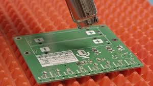
What is the minimum trace width for a PCB prototype?
In addition to the current load, the temperature rise is another critical factor when determining the minimum trace width. When current flows through a trace, it generates heat, and the trace width must be large enough to dissipate this heat without exceeding the board’s thermal limits. If the temperature rise is too high, the components may be damaged or the board may fail to function properly. The temperature rise can be calculated based on the trace width, the current load, and the properties of the PCB material. For more sensitive designs or applications that require optimal performance, such as high-speed circuits or RF circuits, the minimum trace width must be carefully calculated to prevent excessive heat buildup and ensure the reliability of the PCB prototype.
Another consideration when determining the minimum trace width is the manufacturing process itself. PCB manufacturers have limitations on the smallest trace widths they can produce, depending on their equipment and capabilities. Most modern PCB manufacturers can produce trace widths as small as 3 mils (0.003 inches), but this can vary depending on the technology used. For highly complex PCB prototypes, such as those with dense component layouts or high-speed designs, achieving the necessary trace width while maintaining the required electrical performance may require advanced manufacturing techniques, such as laser etching or high-resolution photolithography.
It is also important to note that trace width is not the only factor that affects the overall performance of a PCB prototype. Other design considerations, such as the trace length, the type of signal being transmitted, and the overall design layout, must also be taken into account. For high-frequency or high-speed circuits, designers must consider additional factors like impedance control, signal integrity, and crosstalk, which can be influenced by the trace width and the overall design of the PCB prototype.
Leave a Reply